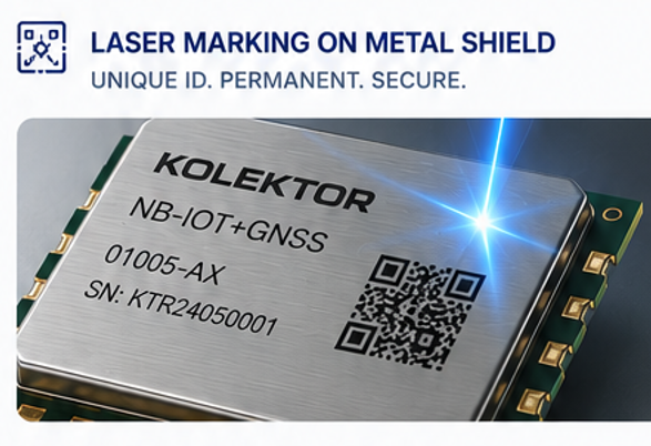
In electronic manufacturing, precision and traceability make all the difference. With the integration of Laser PCB Depanelization and Laser Marking on Metal Shield, it is possible to achieve:
✅ high miniaturization, typical of IoT applications
✅ clean, high-precision cuts
✅ no mechanical stress on the PCB
✅ maximum design freedom
✅ permanent and secure marking
✅ full product traceability
✅ two laser processes in a single line
A solution designed to improve quality, efficiency, and reliability throughout the entire production process